Posts by graysters

Caution: Non registered users only see threads and messages in the currently selected language, which is determined by their browser. Please create an account and log in to see all content by default. This is a limitation of the forum software.


Also users that are not logged in can not create new threads. This is a, unfortunately needed, counter measure against spam. Please create an account and log in to start new threads.

Don't Panic. Please wash hands.

    Right... FPU Sorted!


    It was the FPU socket that was causing the problem!


    Now... Confession time:


    This one was probably my fault for using the FPU socket as a handy place to poke wires into so I could hook it up to my scope while I was debugging the failed CPLD.. Wires that were probably too big and ended up expanding the pin holders in the socket such that a number of them weren't making good contact with the smaller diameter FPU pins when the FPU was in place.


    Anyway, I managed to source a replacement FPU socket, de-solder the old one and replace with the new one. Once in place, not only does the FPU work, it seems to work reliably at a synchronous 55.55MHz... Result!


    Also nice to see Dhrystone is on-par with the '(AC)A1233n-55' benchmark in the module downloaded here: http://wiki.icomp.de/wiki/ACA1233


    One final thing I need to check is the clock port... I'm 99% certain there's a couple of opens from the expansion slot connector to the clock port headers that'll need a couple of patch wires, I'll see if I can source an RTC board to plug in and test.


    Feeling pretty chuffed to have brought this board back to life thanks to Jens' help, and can now sit happy knowing I have one of the fastest 68030 based accelerators ticking away in my A1200 :)


    Cheers,


    Graysters

    As mentioned in my previous post, with the new Data CPLD, it would appear that the CPU and RAM are fully functional on this accelerator. However, I'm not able to get the system to boot with a (multiple) known-good FPU(s) in place.


    I have tried both with a synchronous CPU/FPU clock (55.5MHz), and with the FPU run with a separate crystal at various other frequencies (tried 50MHz, 40MHz, 32MHz, 16MHz, 8MHz)


    Swapping ROMs to DIAGROM, I can see that the system starts OK with the FPU present and clocked, but hangs as soon as it tries to test for the presence of the FPU.


    Looking at the trace above where I'm monitoring pins on the FPU (triggered on !CS going low). Referring to the 68882 datasheet, I *think* the CPU is trying to do a write into the FPU control register (A[4:1]: 0001), and then a read from the FPU response register (A[4:1]: 0000) but I'm a little suspicious of the timing of the various control signals (!CS/!AS/!DS/!DSACK*/R!W), they don't quite tally with the timing diagrams in the datasheet (!AS in particular not going low in the FPU write cycle seems odd...). I've not checked the Data bus yet to see what's happening during the FPU write/read, that's probably my next step... just need to solder some wires to hook my probes onto... any other signals of interest worth probing around the FPU, or CPLDs?


    In the meantime. Jens, I wonder if you would be able to confirm the connectivity of the FPU socket to the CPU, CPLDs, and elsewhere. Anything missing from the connectivity list below that I could check for/patch?


    FPU Pin CPU Pin Data CPLD Address CPLD Other
    CLK - (when solder pad not bridged) - - FPU CLK Crystal Pin
    !CS - - Pin 9 -
    R/!W R/!W Pin 5 Pin 71 -
    !DS !DS - - -
    !AS !AS Pin 72 R12 (Pull-up Res)
    !DSACK0 !DSACK0 - Pin 66 R3 (Pull-up Res)
    !DSACK1 !DSACK1 - Pin 70 R2 (Pull-up Res)
    !SENSE - - Pin 16 -
    !SIZE - - - Tied High
    A0 - - - Tied High
    A1 A1 - Pin 55 (Expansion Connector)
    A2 A2 - Pin 53 (Expansion Connector)
    A3 A3 - Pin 61 (Expansion Connector)
    A4 A4 - Pin 50 (Expansion Connector)
    D31-D0 D31-D0 Various Pins - Various Pins on Bus Driver


    (e.g. is !DS really only connected between CPU and FPU and nowhere else?)


    I couldn't find any connections from the expansion connector FPUCS (pin 115) or FPUSENSE (pin 116) pins, but assumed this is because the FPU is isolated from the amiga bus and only directly coupled to the CPU on the expansion card... (correct me if I'm wrong though!)


    Anywhere else I should go searching for open connections? Specifically in the case where the CPU and RAM appear to work fine, but the FPU doesn't? I did half wonder if there could be a data bus contention issue, whereby when the CPU is trying to read from the FPU, but the Data CPLD is still driving the ACA1233n-55's data bus as I don't know how the the data CPLD distinguishes between a read from the amiga bus or RAM, and the FPU... (presumably lines from the address CPLD to the data CPLD?)


    Your thoughts and insights always much appreciated.


    Cheers,


    Graysters

    Just an update in case anyone was interested in the fate of this card...


    Jens managed to ship me a replacement Data CPLD using his nice carrier board. Here it is with the 'patient':


    I was able to successfully remove the old damaged CPLD and replace it with the new CPLD:


    and, after a bit more debugging (and a couple more patch wires around damaged traces), it lives!


    The CPU on the board appears stable, and all RAM is detected and tests OK! Hooray!


    The one final issue I'm having is getting it working with a known-good FPU (I know... not much software actually uses it... but darn-it do I want this board back fully working!)... but I'll delve into this in the next post...


    Thanks again Jens for the continued above-and-beyond support for his products!


    Cheers,


    Graysters

    Hi Jens,


    I've pinged you a couple of email replies over the past month about this. Assumed you were busy with other stuff, but just in case they weren't getting through, I'm ready to give a CPLD repair board a shot, just contact me when you're ready to arrange the logistics.


    Cheers,


    Graysters

    Hello Jens, me again!


    Just checking in approximately 1 month later to see how the CPLD boards are coming along. Willing customer/tester here, ready and waiting for a aca1233n-55 data flavour CPLD, as and when they're ready!


    No worries if it's going to take some time. I have a poorly A4000/040 on my desk I'm working on to keep me busy while I wait to fix the aca1233n-55!

    Yes, agree this is an academic exercise, more an excuse for me to learn about how these things work whilst sorting out the logistics of a replacement (programmed) part... and giving me an excuse to buy more test gear! That said, the process also uncovered lots of other problems on the board in the mean time, so far from a wasted exercise.


    Totally understand on the remote programming stuff. I'll wait patiently for the CPLD PCB's to arrive. Sounds like the estimate is 'about a month' rather than 'many months', although appreciate customs is the unknown factor here...


    Cheers,


    Graysters

    Right, latest update. the correct JTAG cable arrived today, so I fired up TopJTAG probe and started wiggling pins while monitoring, both on my scope and through the JTAG chain itself).


    Looks like I was in the right ballpark with D31 on the local bus (data CPLD pin 94), but it turns out this side is just fine. Wiggling D31 on the local bus (and all other local data bus pins from the data CPLD) is reflected both externally via scope (measured at the FPU socket), and internally via JTAG chain.


    The problem is actually with D31 on the A1200 bus side of the CPLD. Pin 52 to be precise. I've not exhaustively tested all pins of this bus, but of the pins I have tested, wiggling is reflected externally (seen on scope) and internally (seen on JTAG chain) on all pins *EXCEPT* D31.


    Driving D31 output high does not result in either the D31 CPLD input going high, nor is there any movement externally (measured at the expansion slot):


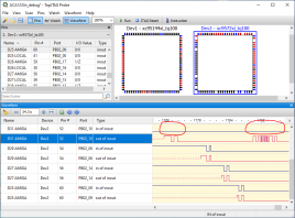
    (Red circles show where I'd expect to see the activity on the output trace reflected, but clearly don't)


    Just for fun, I also tried driving the (tristated) D31 pin with nearby D27, just to see if it was only the output driver, or also input receiver part of the I/O circuit that had died...


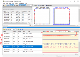
    No movement on the D31 CPLD input, but wiggling was now observed on my scope at D31 on the expansion slot which tells me it's not a short to ground on the board... So, it looks like both input/output paths on Data CPLD pin 52 are dead! That certainly tallies with my earlier observation that transfers from the A1200 bus to the local bus were missing D31, it's just the failure was on the way into the CPLD, not out of it.


    So yes, I guess the short version is 'Yep data CPLD definitely dead!'... cause of death?.... if I had to guess... maybe a rather catostophic ESD event on that pin when the previous owner shifted it between machines?


    Sorry for the long winded waffling debug log. But hopefully the failure analysis may be of some use.


    I'll now eagerly await availability of your mini CPLD boards in order to get hold of a replacement data CPLD... Unless you would be willing to give a secure remote-programming session a go? Let me know and I'll get my fresh XC9572XL soldered on!


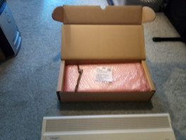
    As an aside... the packaging for the *single* XC9572XL CPLD I ordered is seriously impressive/overkill...
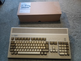
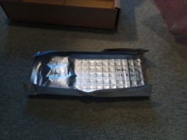


    (A1200 for scale... :) )


    That's a whole 90 capacity IC tray vaccum packed with dessicant for a single CPLD! I guess that's the IC travel equivilent of turning up for a flight and being bumped up to first class on an empty plane!


    All the best,


    Graysters

    Also, I decided to put that small rectangle in the center of the production panel to good use:


    This little board lets me apply power with aligator clips on the mount holes and program a CPLD (44- or 100-pin, not both at the same time) with JTAG. I can then sell the whole board with CPLD as spare part - in your case with a programmed Data CPLD. Only power and JTAG pins are open in the stencil, so de-soldering is easier. The whole thing is flat enough to be shipped in a normal envelope, maybe even slipping through customs.


    What an awesome idea Jens!


    Sign me up straight away as a beta tester/customer number one for this!


    I was ruminating on how best to get a new, programmed data CPLD for this board, given that returns from the UK are a pain right now (I've spent far longer than I care to admit learning about outward processing relief, and other customs jargon before concluding that the system appears broken for an individual using standard couriers)


    I actually bought a replacement XC9572XL to check the feasibility of me paying you to remotely program the thing over a VPN, whilst keeping the jed file secure. It looks doable and is a supported feature of iMPACT (i.e. I setup the JTAG programmer connected to the board here, and run cse_server, you run iMPACT at your end and point it to my IP address:

    https://www.xilinx.com/support…_remote_configuration.htm


    Appreciate this would only be a one-off though and isn't relly scalable to other customers (like your plan is!)


    Cheers,


    Graysters

    Aha, interestingly that one is open too. I'll double check this, and try and locate the open. I've already patched a couple of vias that were open and filled with that copper-oxide looking green gunk, so suspect one of those is the culprit. Couldn't see a trace from the data cpld, but guess it runs under the chip and via's out underneath it

    Now fixed... The open via was under the (now well and truly voided!) warranty label. No change in overall system behaviour though.


    Am I right in saying there are three signals making the serial link between the CPLDs? So far I've found:


    Data CPLD Pin
    Address/Clock CPLD Pin
    #3 #17
    #4
    #95 (now fixed)
    #97 #2


    I assume one of those is a clock (seperate to the main CPU clock) driving the data CPLD, as I couldn't find a connection from the Address/Clock CPLD CPU/FPU clock output (pin 58) to the data CPLD.


    That sounds like water - you don't need aggressive flux to oxidize copper to a degree where it gets green and non-conductive. Still, with the vias covered with solder stop, I wouldn't even expect too much trouble even if the previous owner tried to clean the board with water.

    Could be water I suppose. The problem is that it appears in some places on the board, the solder stop doesn't completely cover the centre of the via, and you get a tiny hole through which the flux/water can enter. the worst affected vias, and where I've found the opens, are those that were underneath the clear labels holding the patch wires down. I guess the liquid wicked underneath the label and was trapped in the vias with no easy way to evaporate away.

    Pin#4 is connected through R13 to Pin#95 of the '144.

    Aha, interestingly that one is open too. I'll double check this, and try and locate the open. I've already patched a couple of vias that were open and filled with that copper-oxide looking green gunk, so suspect one of those is the culprit. Couldn't see a trace from the data cpld, but guess it runs under the chip and via's out underneath it...


    Your bodge wire connects CPU clock to FPU clock. That's not a standard connection; the FPU clock is only equal to CPU clock if you close the FPU clock solder-jumper on the top side of the board (just above the oscillator space). If the oscillator is assembled, then you're shorting the oscillator-out with the clock-output of the main CPLD, possibly damaging the '144.


    I made the connection this side and have bridged the FPU clock jumper for simplicity, and to allow easy probing of clock at the FPU socket, so for now on this board FPU clock=CPU clock. Totally agree that adding an oscillator for the FPU in this config will likely break something, so shaln't be done. Helpfully, the 12V supply wire for the existing 55.5MHz crystal going through the pin-hole prevents addition of this, so we're safe for now. I may rewire this 'properly' to the CPLD output side of the FPU jumper once everything is up and running.


    Local D31 flappin' in the breeze at least indicates "not shorted anywhere". Or is that yellow noise line not D31, but the flat green one?


    Flat green (logic 0) one is D31. The yellow 'noise' one is actually the clock on analog channel 1 (as measured at the FPU pin) It looks like noise as time base is at 5us/division, zoomed in it's much cleaner.


    I think I found all those connections on my first pass, but will go and double check all of them, and check for any shorts to anything nearby.


    (and sometimes even with Keelog/Electroware PSUs, which I highly recommend to send back due to false advertising claims)

    Those things aren't going anywhere near my Amigas.


    All those open connections on your baord are weird. I don't see that the CPU has been removed (or at least it was very nicely soldered back). I have no idea how so many traces could fail - even if some aggressive cleaning fluid had been used, the solder stop should have protected the board.


    Isn't it just weird?! I wonder if the previous owner made an attempt to remove the CPU after an initial problem with the board, maybe they couldn't desolder all the pins (problems heating up ground planes etc.) and gave up, leaving a liberal amount of aggressive flux on the board and under the CPU...


    Naturally, none of this was disclosed by the seller, it was claimed the board was working up until the regulator was knocked off fiting in a new case... That's clearly not the whole story, and I guess my fault for being too trusting. but makes me all the more determined to get this up and running...

    Pins and routing space in the CPLDs are always scarce, although the Xilinx 9500XL series has LOTS of resources if you compare to other vendors. ANDing the two function code lines gives me a "CPU access" signal, cutting lots of equations in the SD-Ram controller and the async access controller in half, as they often have a "not CPU access" term.

    Clever! Sounds like it's well worth the board space for a commonly used term!


    However, I frequently end up with about twice the size of manual routing/placing instructions in the source compared to the actual logic, because chip utilization is so high. The fitter will find a fit after hours of attempting, but that usually doesn't meet timing.


    Even Peter is often baffled by the amount of functionality I can cram into these chips with manual routing, and he's our master of making low-cost FPGAs do things at speeds that are often only possible with the next-higher speed grade

    Consider me impressed! I've not played with manual routing on CPLDs. But I've been pleased with how much functionality you can squeeze into these things. A previous project I was on required the use of a CPLD to both convert an incoming SPI bitstream on the fly (signed->2s compliment) and seperately monitor another serial output for a 4 bit number representing a detected 'keyword' (this was an increadibly low power ASIC speech recognition demo). The initial spec used the smallest coolrunner-II CPLD from Xilinx, and was only going to display a hex number representing which of the 16 words were detected, but with some heavily optimised verilog, I was able to (only just!) fit in a fairly sophisticated text scroller in there that pulled and displayed the exact word from a lookup table! :)


    "down there" it's only data lines and clock port stuff that's 1:1 from the connector. Most (if not all) of the connections are direct to the CPLD, and I have my doubts that you find a bad connection there

    Understood, and I think I've traced everything to the data CPLD anyway. The only functional pin on the data CPLD I can't find connected is pin 4 (function block2, cell 2 of the CPLD), all others appear used, or specified N/C in the datasheet.


    Anyway... some further progress...


    Thanks to your PCB image, I've identified and fixed (I believe) all the opens around the CPU pins, which were:


    D1

    D13

    D18

    D19

    FC0 (not FC1 as mentioned on Friday, that one was fine!)

    DSACK0

    A30

    and wait for it...

    CLK.. (Seriously... I *really* should have spotted this one sooner!! :rolleyes:)


    I also found and fixed an open on D28 from the expansion slot to the data CPLD (shown in topside board pic below).


    At this point we've now progressed to a red screen when powering on the A1200 (previously black screen), so I've fired up my shiny new Rigol MSO1104Z and started probing around at power-on. I'm seeing lots of activity on the address/data strobes and data lines on both A1200 bus, and on the local 32bit bus, which would seem to confirm at least a semi-functional Data CPLD routing stuff back and forth. However the first potential Data CPLD issue I see is on D31 on the local bus where I'm seeing no activity (constant logic 0). All other data pins seem to mirror exactly what is seen across both busses (i.e. A1200 D0 = Local Bus D0, A1200 D1 = Local bus D1 etc..) Changes on the A1200 bus D31 do not appear on the local bus D31. I've checked for shorts on this pin to VDD/Ground, and it appears isolated.

    (note pulses on the A1200 bus D31 are not reflected on the local bus D31, whereas D25 and D27 match across the busses)


    Unless there's something special about the upper-most data bit on the local bus, my current working theory is that some part of the I/O driver on this pin in the CPLD (pin 94, function block2, cell 2. Shown below) is shorted internally and sinking a load of current (hence the heat given off). I'll be able to confirm once the right JTAG cable arrives and I can try specifically wiggling this pin...


    (Suspect CPLD Pin highlighted, A1200 Bus D28 bodge wire also shown!)


    Anything else worth checking/probing for while I wait for this (second!) JTAG cable?


    Thanks as always,


    Graysters

    That's because the "highest address line" can be selected with R11 or R10: R11 will pass A30 to the controller CPLD, and R10 will pass A27. This allowed me to check the ACA1233n design with the ACA1233 CPLD code before I started developing the Z3 autoconfig part, which is implemented "kinda weird", as it's distributed over two CPLDs with a serial link between the two. In development, you want to test in small steps (called "unit testing", but already practised by Werner von Braun when he sent the first rockets to space).

    That makes perfect sense. Building on something that's known working, one step at a time. So if (when) something breaks, you limit the scope of what you need to debug.


    Right, I won't open the schematics, but this should help you tracing/repairing connections


    Jens, Thank you so much for this. that helps enormously, and confirms a couple of suspicions around unused pins, and also that FC1 CPU pin is currently open and needs patching.

    I noticed that FC0 and (I suspected, but I now know FC1) go to the discrete AND gate U14 before heading into the CPLD... so did you run out of pins, or logic in that CPLD? ;)


    One last request for now... could you share the same style image, but showing the lower half of the expansion port connection (just to check for opens that may be lurking under the plastic connector?


    Thanks again! This is really first rate support!


    Best Regards,


    Graysters